In printed circuit board manufacturing, having a PCB with reliable electrical performance, mechanical integrity, and overall durability is required. One of the ways PCB manufacturers achieve these properties in their products is through PCB edge plating. This process ensures that connections remain robust and reliable which is why it is a standard practice in advanced PCB design and production.
In this article, we will discuss more about the PCB edge plating process. We will explore a comprehensive guide to the process, its benefits, materials, and key considerations to give you a better understanding about it and how you might do it effectively.
What is PCB Edge Plating?
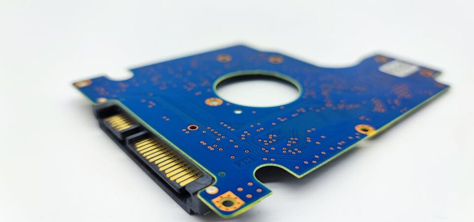
This is also known as edge castellation or plated edges. It is the process of depositing a copper layer along the edges of a printed circuit board. This layer typically extends from the top and bottom layers to the sidewalls of the board, creating a seamless electrical path.
The edge plating process ensures that the connections between different layers of the PCB are well-protected and reliable, particularly in complex circuit applications.
Edge plating is particularly critical in high-frequency and high-power applications where maintaining signal integrity is paramount.
Materials Used in PCB Edge Plating
To ensure optimal performance, this process requires the use of highly conductive and durable materials. The most common ones used are copper, nickel, and gold.
Copper acts as the primary conductive material that establishes the electrical connection and provides mechanical strength.
Nickel is applied as a layer acting as a diffusion barrier between copper and the final plating layer.
Although there are many other alternatives to the final layer in the PCB edge plating process, gold is often used because of its excellent conductivity, corrosion resistance, and durability properties.
The plating thickness depends on the specific requirements of the design. A thicker plating ensures better mechanical strength while thinner plating is ideal for lower-stress applications.

PCB Edge Plating Process Step-by-Step
This process involves several steps to ensure precision and consistency. Below is a detailed breakdown of the process:
1. Board Design and Preparation
The edge plating process begins at the design stage. Engineers must clearly specify which edges of the PCB require plating. This information is incorporated into the Gerber files or other CAD documentation, which guide the manufacturing process.
2. Copper Plating
Once the PCB board is manufactured and drilled, the initial copper plating is applied. This process involves electroplating copper onto the entire circuit board, including the edges that will undergo further plating.
3. Edge Beveling
To prepare the edges for PCB edge plating, the board undergoes a beveling or routing process. This step smooths the edges and ensures they are free of burrs or irregularities. Proper edge preparation is critical to achieving uniform plating thickness.
4. Surface Treatment and Masking
Before the PCB edge plating process, areas of the board that do not require plating are masked off. The remaining exposed circuit layers, including the edges, are chemically cleaned to remove any contaminants or oxides.
5. Electroplating Process
The prepared PCB is placed in an electroplating bath. A layer of copper is electroplated onto the edges of the board, ensuring electrical continuity between the surface layers and the plated edges. If necessary, additional layers of nickel and gold are applied sequentially.
The plating process during PCB edge plating is carefully monitored to achieve the desired thickness and uniformity across the edges.
6. Quality Inspection
After plating, the PCB undergoes a thorough inspection to ensure the integrity of the plated edges. This includes checking for uniform plating thickness, electrical continuity, and adherence to design specifications.
PCB Edge Plating Services
Edge plating is essential for applications like high-frequency circuit boards, connectors, power electronics, and aerospace, offering significant benefits. However, reliability is key.
At Alternate Finishing, Inc., we specialize in metal plating services – including reliable edge plating – for customers in the US and Canada across various industries. Our experienced team ensures quick turnarounds and dependable results.
With a reliable PCB edge plating process from Alternate Finishing, Inc., your PCBs will be able to meet the demands of even the most challenging environments. For edge plating or any metal finishing services, call us for a quote.


